Logic Controller
There is no software available. Currently there is only hardware design available.
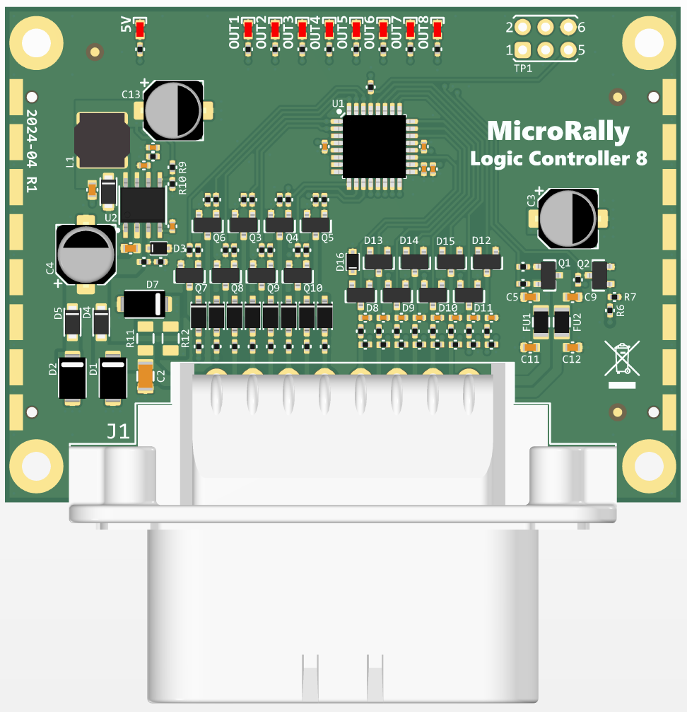
A programmable device with 8 inputs and 8 outputs. Inputs are be 5V analog inputs, and outputs are Open-drain (low-side) type. This way you can control relays using buttons, not switches. Or have some logic that combines multiple inputs to control single output. Or simulate switch using buttons that latch state. One use case is steering wheel button interface. Device is be based on a simple ATmega328PB controller. That way it should be easy to make any logic you want.
Pinout
Connector - TE Connectivity Ampseal series, 23pins
PCB header part# - 770669-x (x - key)
Amperage - 7.5A/pin
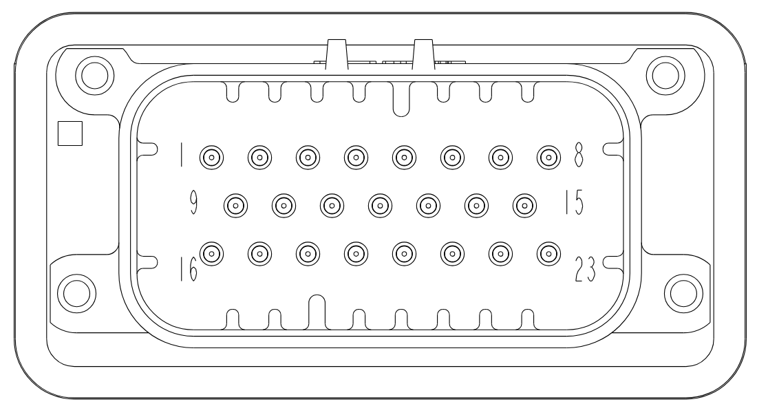
| Pin# | Signal | Description | Type |
|---|---|---|---|
| 1 | VABT | Battery power | P |
| 2 | OUT1 | Output 1 | OD |
| 3 | OUT2 | Output 2 | OD |
| 4 | OUT3 | Output 3 | OD |
| 5 | IN1 | Input 1 | AIN |
| 6 | IN2 | Input 2 | AIN |
| 7 | IN3 | Input 3 | AIN |
| 8 | 5V_OUT | 5V Output | PO |
| 9 | VIGN | Enable power | P |
| 10 | OUT4 | Output 4 | OD |
| 11 | OUT5 | Output 5 | OD |
| 12 | GND | Ground | P |
| 13 | IN4 | Input 4 | AIN |
| 14 | IN5 | Input 5 | AIN |
| 15 | 5VSW | Switched 5V output | PO |
| 16 | GND | Ground | G |
| 17 | OUT6 | Output 6 | OD |
| 18 | OUT7 | Output 7 | OD |
| 19 | OUT8 | Output 8 | OD |
| 20 | IN6 | Input 6 | G |
| 21 | IN7 | Input 7 | AIN |
| 22 | IN8 | Input 8 | AIN |
| 23 | GND | Ground | G |
P - Power input, 12V
G - Ground, 0V
PO - Power output, 5V
OD - Open-drain output, 12V, switched to ground
AIN - Analog input, 5V
Connections
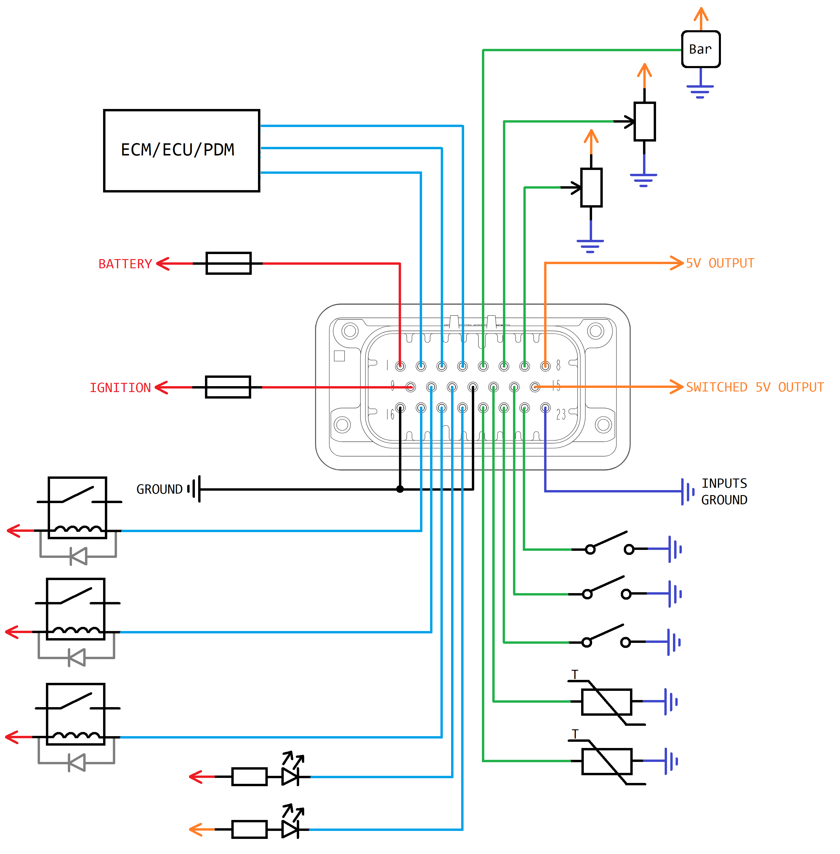
Example of possible connections.
Outputs
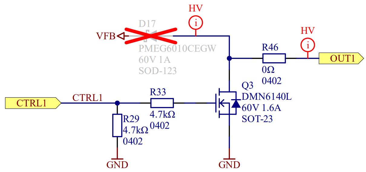
This is schematic of one output channel.
Each output is capable of sinking 1.5A of current. Each output has a place for resistor that can act as one time fuse in case of excessive overparent. Adjust this value as needed. All outputs are switched to common ground.
Relays - when controlling relays (or any other inductive load), it is highly recommended to add flyback diode accross relay coil. This way there will be no possibility of a high voltage spike, that could permanently damage output of logic controller.
Additionally every output can be equipped with a flyback diode, that protects against high voltage spike during inductive load turn-off. By default it's not soldered, because special consideration has to be taken to use them. Primary concern is back-feeding. Built in flyback diodes can be used only if all loads are supplied from single supply source, like a battery. If possible it's better to use external flyback diodes.
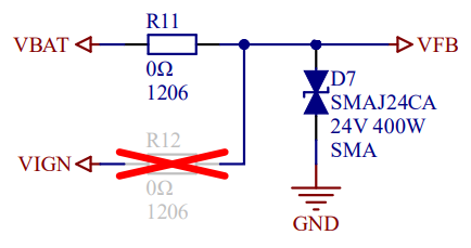
If built-in diodes are used, then choose appropriate return supply with R11 and R12 resistors.
It is also possible to choose none, and completely relay on D7 TVS diode. This way there are no risks of back-feeding, but total suppression capability is limited by this one component.
Inputs
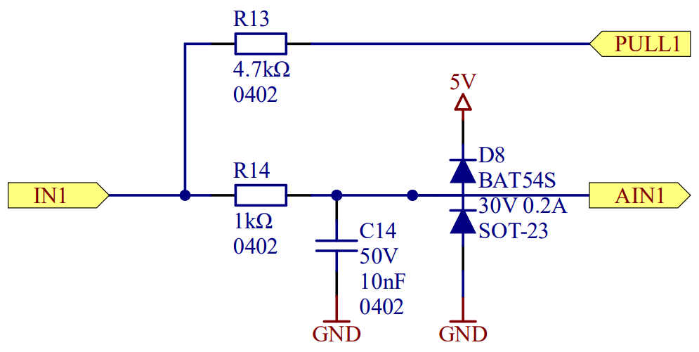
This is schematic of one input channel.
Maximum rated input voltage of any input is 5.6V, higher voltages may cause permanent damage to input or whole device. There are input protection circuits, but their capabilities are limited, so it's better to avoid signals that are outside of -0.6V to +5.6V range.
Each output has software controllable pull resistor. It can be either pull-down or pull-up or left floating. Default value of this resistor is 4.7kΩ. Change it as it suits your application. Other signal is analog input that is protected with 1kΩ resistor and diodes. Also there is a small capacitor, that forms low-pass filter for noise suppression or debounce for switches.
Ground
Input devices can be connected to chassis ground, as all ground pins are internally connected and device will work just fine with only one of them connected. But for analog sensors it is highly recommended to use separate inputs ground, to mitigate ground offsets. But be mindful of ground loops that can occur, if sensors body is no isolated from internal circuitry.